CUDA 存储体系结构
概述
In general, applications do not access arbitrary data or run arbitrary code at any point-in-time. Instead, applications often follow the principle of locality, which suggests that they access a relatively small and localized portion of their address space at any point-in-time. There are two different types of locality:
- Temporal locality (locality in time)
- Spatial locality (locality in space)
Temporal locality assumes that if a data location is referenced, then it is more likely to be referenced again within a short time period and less likely to be referenced as more and more time passes. Spatial locality assumes that if a memory location is referenced, nearby locations are likely to be referenced as well.
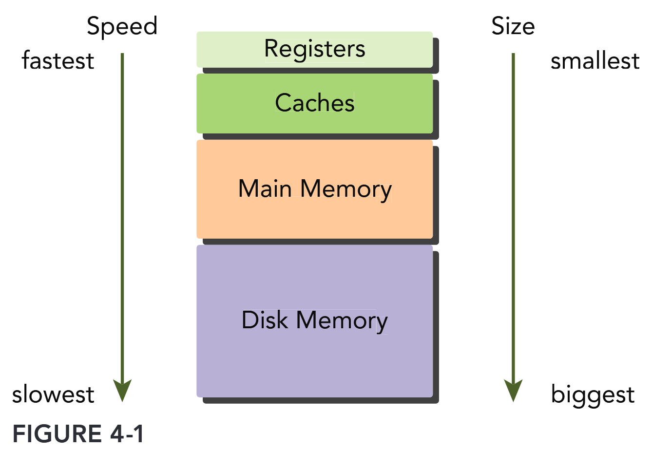
Modern computers use a memory hierarchy of progressively lower-latency but lower-capacity memories to optimize performance. This memory hierarchy is only useful because of the principle of locality. A memory hierarchy consists of multiple levels of memory with different latencies, bandwidths, and capacities.
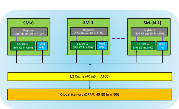
Both GPUs and CPUs use similar principles and models in memory hierarchy design. The key difference between GPU and CPU memory models is that the CUDA programming model exposes more of the memory hierarchy and gives you more explicit control over its behavior.
CUDA 存储体系结构
To programmers, there are generally two classifications of memory:
- Programmable: You explicitly control what data is placed in programmable memory.
- Non-programmable: You have no control over data placement, and rely on automatic techniques to achieve good performance.
In the CPU memory hierarchy, L1 cache and L2 cache are examples of non-programmable memory. On the other hand, the CUDA memory model exposes many types of programmable memory to you:
- Registers
- Shared memory
- Local memory
- Constant memory
- Texture memory
- Global memory
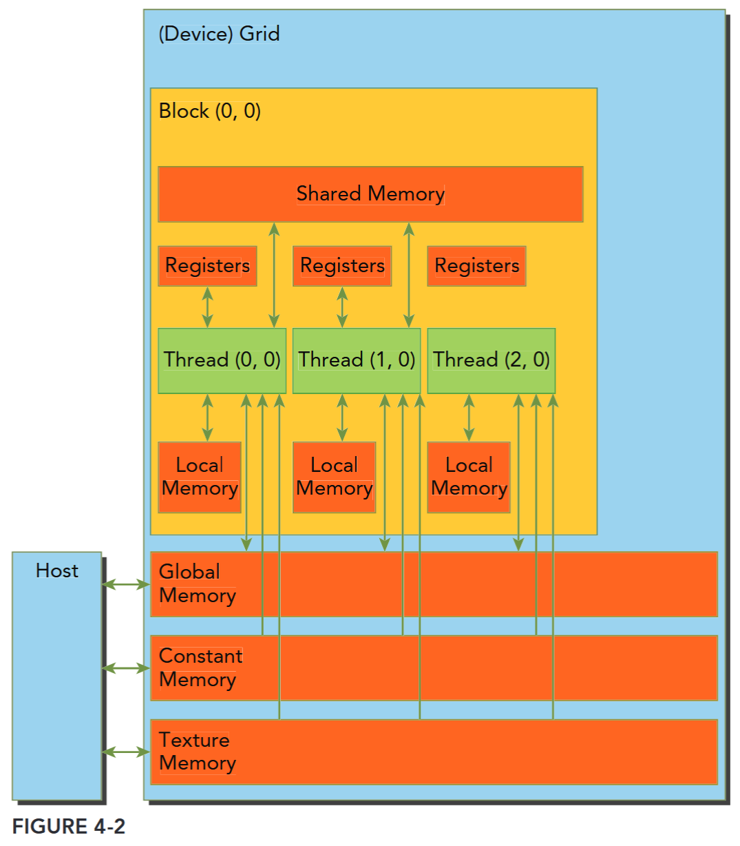
每个层次都有不同的范围、生命周期、缓存行为。CUDA 线程在执行期间可以从多种内存空间中访问数据,可以看到:
- 每个线程有自己的私有本地内存(Local Memory),
- 而每个线程块有包含共享内存(Shared Memory), 该共享内存内存对该块中的所有线程可见,并且具有与该块相同的生命周期。
- 线程块集群中的线程块可以对彼此的共享内存执行读取、写入和原子操作。
- 所有线程都可以访问相同的全局内存(Global Memory)。
- 还有两个额外的只读内存空间可供所有线程访问:常量内存(Constant Memory)和纹理内存(Texture Memory)。
全局、常量和纹理内存空间针对不同的内存使用进行了优化(Device Memory Accesses)。纹理内存还为某些特定数据格式提供了不同的寻址模式以及数据过滤方法(Texture and Surface Memory)。全局、常量、纹理内存有和应用相同的生命周期,也即全局内存、常量内存和纹理内存空间在同一应用程序启动的不同内核(kernel)之间是持久存在的。 简单来说,就是当同一个应用程序多次启动内核去执行任务时,这几种内存里的数据不会因为内核的启动和结束而消失,会一直保持着,方便后续内核继续使用这些内存中的数据。

Registers
其中寄存器是 GPU 上运行速度最快的内存空间,通常其带宽为 8TB/s 左右,延迟为 1 个时钟周期。核函数中声明的一个没有其他修饰符的自变量,通常就存储在寄存器中。最快速也最受偏爱的存储器就是设备中的寄存器,属于具有重要价值有极度缺乏的资源。
Registers are the fastest memory space on a GPU. An automatic variable declared in a kernel without any other type qualifiers is generally stored in a register. Arrays declared in a kernel may also be stored in registers, but only if the indices used to reference the array are constant and can be determined at compile time.
Register variables are private to each thread. A kernel typically uses registers to hold frequently accessed thread-private variables. Register variables share their lifetime with the kernel. Once a kernel completes execution, a register variable cannot be accessed again.
Registers are scarce resources that are partitioned among active warps in an SM. Using fewer registers in your kernels may allow more thread blocks to reside on an SM. More concurrent thread blocks per-SM can increase occupancy and improve performance.
max registers/thread: Fermi: 63, Kepler: 255, V100/A100/H100: 255 (See Also whitepaper)
使用
nvcc编译加上-Xptxas -v或--resource-usage查看使用的寄存器、共享内存等信息(See also ptxas options)。
If a kernel uses more registers than the hardware limit, the excess registers will spill over to local memory. This register spilling can have adverse performance consequences. The nvcc compiler uses heuristics to minimize register usage and avoid register spilling. You can optionally aid these heuristics by providing additional information for each kernel to the compiler in the form of launch bounds:
__global__ void
__launch_bounds__(maxThreadsPerBlock, minBlocksPerMultiprocessor, maxBlocksPerCluster)
MyKernel(...) { ... }
maxThreadsPerBlock specifies the maximum number of threads per block that a kernel will launch. minBlocksPerMultiprocessor is optional, and specifies the desired minimum number of resident blocks per SM. Optimal launch bounds for a given kernel will usually differ across major architectural revisions.
You can also control the maximum number of registers used by all kernels in a compilation unit using the maxrregcount compiler option. In this example: -maxrregcount=32. the value specified (32) is ignored for any kernels that have launch bounds specified.
Local Memory
Variables in a kernel that are eligible for registers but cannot fit into the register space allocated for that kernel will spill into local memory. Variables that the compiler is likely to place in local memory are:
- Local arrays referenced with indices whose values cannot be determined at compile-time.
- Large local structures or arrays that would consume too much register space.
- Any variable that does not fit within the kernel register limit. The name “local memory” is misleading: Values spilled to local memory reside in the same physical location as global memory, so local memory accesses are characterized by high latency and low bandwidth and are subject to the requirements for efficient memory access that are described in the section “Memory Access Patterns” found later in this chapter. For GPUs with compute capability 2.0 and higher, local memory data is also cached in a per-SM L1 and per-device L2 cache.
Local memory 物理位置在 global memory。
Shared Memory
接下来是共享内存,共享内存是 GPU 上可受用户控制的一级缓存。共享内存类似于 CPU 的缓存,不过与 CPU 的缓存不同,GPU 的共享内存可以有 CUDA 内核直接编程控制。由于共享内存是片上内存,所以与全局内存相比,它具有更高的带宽与更低的延迟,通常其带宽为 1.5TB/s 左右,延迟为 1~32 个时钟周期。对于共享内存的使用,主要考虑数据的重用性。当存在着数据的重复利用时,使用共享内存是比较合适的。如果数据不被重用,则直接将数据从全局内存或常量内存读入寄存器即可。
Variables decorated with the following attribute in a kernel are stored in shared memory: __shared__.
Because shared memory is on-chip, it has a much higher bandwidth and much lower latency than local or global memory. It is used similarly to CPU L1 cache, but is also programmable. Each SM has a limited amount of shared memory that is partitioned among thread blocks. Therefore, you must be careful to not over-utilize shared memory or you will inadvertently limit the number of active warps.
Shared memory is declared in the scope of a kernel function but shares its lifetime with a thread block. When a thread block is finished executing, its allocation of shared memory will be released and assigned to other thread blocks.
Shared memory serves as a basic means for inter-thread communication. Threads within a block can cooperate by sharing data stored in shared memory. Access to shared memory must be synchronized using the following CUDA runtime call introduced in earlier chapters: void __syncthreads();. This function creates a barrier which all threads in the same thread block must reach before any other thread is allowed to proceed. By creating a barrier for all threads within a thread block, you can prevent a potential data hazard.
They occur when there is an undefined ordering of multiple accesses to the same memory location from different threads, where at least one of those accesses is a write. —syncthreads may also affect performance by forcing the SM to idle frequently.
Configuration of shared memory and L1 cache see also Configuring the Amount of Shared Memory
Constant Memory & Texture Memory
Constant memory resides in device memory and is cached in a dedicated, per-SM constant cache. A constant variable is decorated with the following attribute: __constant__. Constant variables must be declared with global scope, outside of any kernels. A limited amount of constant memory can be declared — 64 KB for all compute capabilities. Constant memory is statically declared and visible to all kernels in the same compilation unit.
Kernels can only read from constant memory. Constant memory must therefore be initialized by the host using:
cudaError_t cudaMemcpyToSymbol(const void* symbol, const void* src, size_t count);
// https://docs.nvidia.com/cuda/cuda-runtime-api/group__CUDART__MEMORY.html#group__CUDART__MEMORY_1g9bcf02b53644eee2bef9983d807084c7
This function copies count bytes from the memory pointed to by src to the memory pointed to by symbol, which is a variable that resides on the device in global or constant memory. This function is synchronous in most cases. Constant memory performs best when all threads in a warp read from the same memory address. For example, a coefficient for a mathematical formula is a good use case for constant memory because all threads in a warp will use the same coefficient to conduct the same calculation on different data. If each thread in a warp reads from a different address, and only reads once, then constant memory is not the best choice because a single read from constant memory broadcasts to all threads in a warp.
Texture memory resides in device memory and is cached in a per-SM, read-only cache. Texture memory is a type of global memory that is accessed through a dedicated read-only cache. The readonly cache includes support for hardware filtering, which can perform floating-point interpolation as part of the read process. Texture memory is optimized for 2D spatial locality, so threads in a warp that use texture memory to access 2D data will achieve the best performance. For some applications, this is ideal and provides a performance advantage due to the cache and the filtering hardware. However, for other applications using texture memory can be slower than global memory.
Global Memory
全局内存是 GPU 中最大、延迟最高并且最常使用的内存。全局内存类似于 CPU 的系统内存。在编程中对全局内存访问的优化以最大化程度提高全局内存的数据吞吐量是十分重要的。
The name global refers to its scope and lifetime. Its state can be accessed on the device from any SM throughout the lifetime of the application. A variable in global memory can either be declared statically or dynamically. You can declare a global variable statically in device code using the following qualifier: __device__.
Global memory allocations exist for the lifetime of an application and are accessible to all threads of all kernels. You must take care when accessing global memory from multiple threads. Because thread execution cannot be synchronized across thread blocks, there is a potential hazard of multiple threads in different thread blocks concurrently modifying the same location in global memory, which will lead to an undefined program behavior.
Global memory resides in device memory and is accessible via 32-byte, 64-byte, or 128-byte memory transactions. These memory transactions must be naturally aligned; that is, the first address must be a multiple of 32 bytes, 64 bytes, or 128 bytes. Optimizing memory transactions are vital to obtaining optimal performance. When a warp performs a memory load/store, the number of transactions required to satisfy that request typically depends on the following two factors:
- Distribution of memory addresses across the threads of that warp.
- Alignment of memory addresses per transaction.
In general, the more transactions necessary to satisfy a memory request, the higher the potential for unused bytes to be transferred, causing a reduction in throughput efficiency. For a given warp memory request, the number of transactions and the throughput efficiency are determined by the compute capability of the device.
GPU Caches
Like CPU caches, GPU caches are non-programmable memory. There are four types of cache in GPU devices:
- L1
- L2
- Read-only constant
- Read-only texture
There is one L1 cache per-SM and one L2 cache shared by all SMs. Both L1 and L2 caches are used to store data in local and global memory, including register spills. On Fermi GPus and Kepler K40 or later GPUs, CUDA allows you to configure whether reads are cached in both L1 and L2, or only in L2. On the CPU, both memory loads and stores can be cached. However, on the GPU only memory load operations can be cached; memory store operations cannot be cached. Each SM also has a read-only constant cache and read-only texture cache that are used to improve read performance from their respective memory spaces in device memory.
注意 GPU 的 Cache 行为的一些特殊性质。
合理使用总结
下表对各个存储层次进行总结:
| 存储类型 | 容量 | 延迟 | 带宽 | 访问权限 | 适用场景 |
|---|---|---|---|---|---|
| 寄存器 | 每个线程 KB 级 | ~1 周期 | 无限 | 线程私有 | 高频临时变量 |
| 共享内存 | 每个 SM 96KB | ~10 周期 | ~1TB/s | 块内共享 | 数据重用(如矩阵乘 tiling) |
| 常量内存 | 64KB | ~20 周期 | ~800GB/s | 全局只读 | 频繁访问的常量数据 |
| 全局内存 | GB 级 | ~400 周期 | ~1TB/s | 全局读写 | 大数据存储 |
| 纹理内存 | GB 级 | ~320 周期 | ~800GB/s | 只读,优化 2D 访问 | 图像 / 视频处理 |
- 寄存器:优先存放循环变量、计算中间值
→ 避免寄存器溢出(通过
nvcc --ptxas-options=-v查看) - 共享内存:手动管理数据缓存
__shared__ float tile[32][32]; // 矩阵乘分块- 全局内存:确保合并访问(Warp 内连续线程访问连续地址)
→ 例如:
float4类型访问比float效率高 4 倍
TABLE 4-1: CUDA Variable and Type Qualifier
| QUALIFIER | VARIABLE NAME | MEMORY | SCOPE | LIFESPAN |
|---|---|---|---|---|
| float var | Register | Thread | Thread | |
| float var[100] | Local | Thread | Thread | |
__shared__ | float var† | Shared | Block | Block |
__device__ | float var† | Global | Global | Apllication |
__constant__ | float var† | Constant | Global | Application |
† can be either scalar variable or array variable
TABLE 4-2: Salient Features of Device Memory
| MEMORY | ON/OFF CHIP | CACHED | ACCESS | SCOPE | LIFETIME |
|---|---|---|---|---|---|
| Register | On | n/a | R/W | 1 thread | Thread |
| Local | Off | † | R/W | 1 thread | Thread |
| Shared | On | n/a | R/W | All threads in block | Block |
| Global | Off | † | R/W | All threads + host | Host allocation |
| Constant | Off | Yes | R | All threads + host | Host allocation |
| Texture | Off | Yes | R | All threads + host | Host allocation |
† Cached only on devices of compute capability 2.x
VARIABLES IN FILE SCOPE: VISIBLE VERSUS ACCESSIBLE
这一章节的内容可能发生变化,需要重新审查
In CUDA programming, you work in two distinct worlds: the host and the device. In general, device kernels cannot access host variables and host functions cannot access device variables, even though these variables are declared in the same file scope. The CUDA runtime API can access both host and device variables, but it is up to you to provide the correct arguments to the correct functions so that they operate properly on the correct variables. Because the runtime API makes assumptions about the memory space of certain parameters, passing a host variable where it expects a device variable or vice versa will result in undefined behavior (likely crashing your application).
#include <cuda_runtime.h>
#include <stdio.h>

__device__ float devData;

__global__ void checkGlobalVariable() {
  // display the original value
  printf("Device: the value of the global variable is %f\n", devData);

  // alter the value
  devData += 2.0f;
}

int main(void) {
  // initialize the global variable
  float value = 3.14f;
  cudaMemcpyToSymbol(devData, &value, sizeof(float));
  printf("Host: copied %f to the global variable\n", value);

  // invoke the kernel
  checkGlobalVariable<<<1, 1>>>();

  // copy the global variable back to the host
  cudaMemcpyFromSymbol(&value, devData, sizeof(float));
  printf("Host: the value changed by the kernel to %f\n", value);

  cudaDeviceReset();
  return EXIT_SUCCESS;
}
The following code illustrates how to statically declare a global variable. As shown in Listing 4-1, a global variable of type float is declared with file scope. In the kernel function checkGlobal-Variable, the value of that global variable is printed and then its value is changed. In function main, the value of that global variable is initialized using the function cudaMemcpyToSymbol. After checkGlobalVariable is executed, the value of the global variable is altered. Its new value is then copied back to the host using cudaMemcpyFromSymbol.
Even though the host and device code are stored in the same file, they exist in completely different worlds. The host code cannot directly access a device variable even if it is visible in the same file scope. Similarly, device code cannot directly access a host variable either.
You might argue that the host code in fact can access the device global variable using the following code:
cudaMemcpyToSymbol(devD6ata, &value, sizeof(float));
Yes, but notice that:
- cudaMemcpyToSymbol is in the CUDA runtime API and uses GPU hardware behind the scenes to perform the access.
- The variable devData is passed here as a symbol, not as the address of the variable in device global memory.
- In the kernel, devData is used as a variable in global memory.
cudaMemcpy cannot be used to transfer data into devData using the address of the variable:
// Error
cudaMemcpy(&devData, &value, sizeof(float),cudaMemcpyHostToDevice);
You cannot use the reference operator & on a device variable from the host, because it is simply a symbol representing the physical location on the GPU. However, you can acquire the address of a global variable by explicitly making a call using the following CUDA API:
cudaError_t cudaGetSymbolAddress(void** devPtr, const void* symbol);This function fetches the physical address of the global memory associated with the provided device symbol. After acquiring the address of the variable devData, you then can use the cudaMemcpy function as follows:
float *dptr = NULL;
cudaGetSymbolAddress((void**)&dptr, devData);
cudaMemcpy(dptr, &value, sizeof(float), cudaMemcpyHostToDevice);
There is a single exception to being able to directly reference GPU memory from the host: CUDA pinned memory. Both host code and device code can access pinned memory directly by simply dereferencing a pointer. You will learn about pinned memory in the next section.
Memory Management
Memory management in CUDA programming is similar to C programming, with the added programmer responsibility of explicitly managing data movement between the host and device.
The latest advancements in this area will be covered in this chapter under “Unified Memory.” For now, you will focus on how you can explicitly manage memory and data movement using CUDA functions to:
- Allocate and deallocate device memory
- Transfer data between the host and device
Memory Allocation and Deallocation and Transfer
See also Managing Memory.
The values contained in the allocated global memory are not cleared. It is your responsibility to either fill the allocated global memory with data transferred from the host, or initialize it with the following function: cudaError_t cudaMemset(void *devPtr, int value, size_t count); This function fills each of the count bytes starting at the device memory address devPtr with the value stored in the variable value.
Device memory allocation and deallocation are expensive operations, so device memory should be reused by applications whenever possible to minimize the impact on overall performance.
Pinned Memory
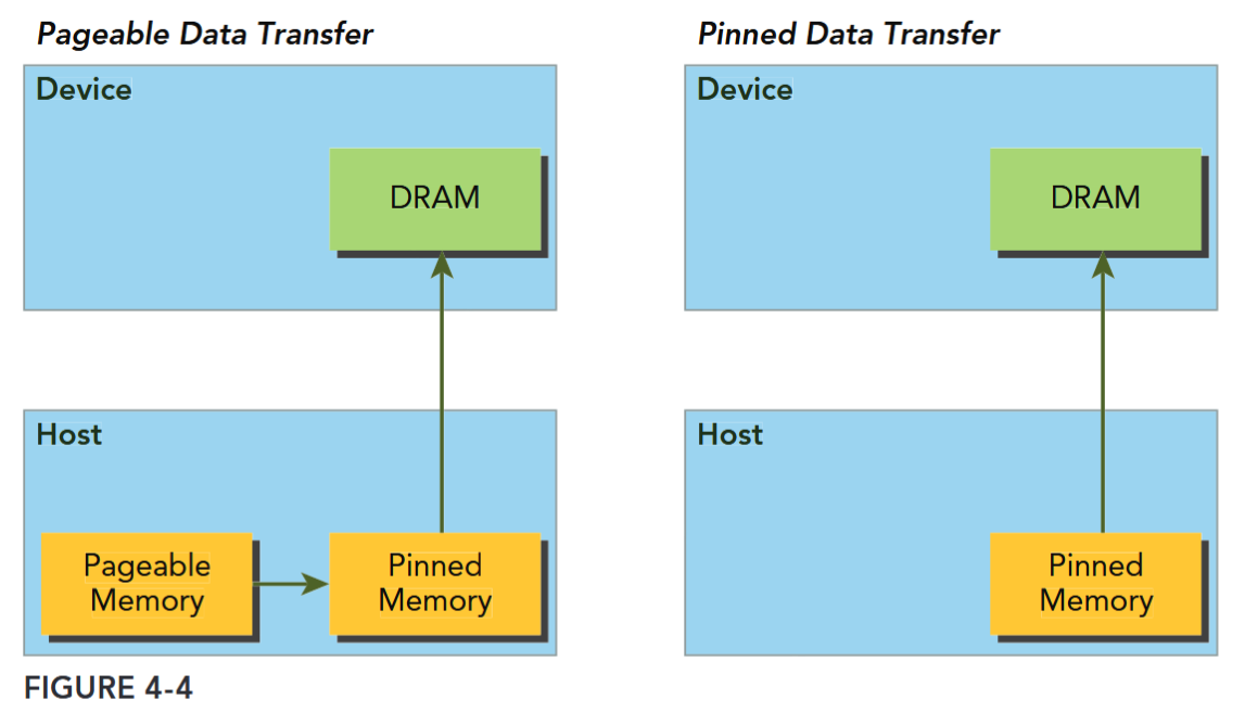
Allocated host memory is by default pageable, that is, subject to page fault operations that move data in host virtual memory to different physical locations as directed by the operating system. Virtual memory offers the illusion of much more main memory than is physically available, just as the L1 cache offers the illusion of much more on-chip memory than is physically available. The GPU cannot safely access data in pageable host memory because it has no control over when the host operating system may choose to physically move that data.
When transferring data from pageable host memory to device memory, the CUDA driver first allocates temporary page-locked or pinned host memory, copies the source host data to pinned memory, and then transfers the data from pinned memory to device memory, as illustrated on the left side of Figure 4-4.
The CUDA runtime allows you to directly allocate pinned host memory using:
__host__ cudaError_t cudaMallocHost ( void** ptr, size_t size )
/*
Allocates page-locked memory on the host.
###### Parameters
ptr
- Pointer to allocated host memory
size
- Requested allocation size in bytes
*/This function allocates count bytes of host memory that is page-locked and accessible to the device. Since the pinned memory can be accessed directly by the device, it can be read and written with much higher bandwidth than pageable memory. However, allocating excessive amounts of pinned memory might degrade host system performance, since it reduces the amount of pageable memory available to the host system for storing virtual memory data.
Pinned host memory must be freed with:
__host__ cudaError_t cudaFreeHost ( void* ptr )
/*
Frees page-locked memory.
###### Parameters
ptr
- Pointer to memory to free
*/MEMORY TRANSFER BETWEEN THE HOST AND DEVICE
Pinned memory is more expensive to allocate and deallocate than pageable memory, but it provides higher transfer throughput for large data transfers. The speedup achieved when using pinned memory relative to pageable memory depends on device compute capability. Batching many small transfers into one larger transfer improves performance because it reduces per-transfer overhead. Data transfers between the host and device can sometimes be overlapped with kernel execution.
Zero-Copy Memory TODO
In general, the host cannot directly access device variables, and the device cannot directly access host variables. There is one exception to this rule: zero-copy memory. Both the host and device can access zero-copy memory.
GPU threads can directly access zero-copy memory. There are several advantages to using zero-copy memory in CUDA kernels, such as:
- Leveraging host memory when there is insufficient device memory
- Avoiding explicit data transfer between the host and device
- Improving PCIe transfer rates
Unified Virtual Addressing
Unified Memory
MEMORY ACCESS PATTERNS
Most device data access begins in global memory, and most GPU applications tend to be limited by memory bandwidth. Therefore, maximizing your application’s use of global memory bandwidth is a fundamental step in kernel performance tuning. If you do not tune global memory usage properly, other optimizations will likely have a negligible effect.
To achieve the best performance when reading and writing data, memory access operations must meet certain conditions. One of the distinguishing features of the CUDA execution model is that instructions are issued and executed per warp. Memory operations are also issued per warp. When executing a memory instruction, each thread in a warp provides a memory address it is loading or storing. Cooperatively, the 32 threads in a warp present a single memory access request comprised of the requested addresses, which is serviced by one or more device memory transactions. Depending on the distribution of memory addresses within a warp, memory accesses can be classified into different patterns. In this section, you are going to examine different memory access patterns and learn how to achieve optimal global memory access.
最大限度地提高应用程序对全局内存带宽的利用率,是内核性能调优的一个基本步骤。
CUDA执行模型的一个显著特点是,指令按线程束(warp)发布和执行。内存操作也是按线程束发布的。在执行内存指令时,线程束中的每个线程都会提供其要加载或存储的内存地址。线程束中的32个线程协同工作,共同提出一个包含所请求地址的内存访问请求,该请求由一个或多个设备内存事务来处理。根据线程束内内存地址的分布情况,内存访问可以分为不同的模式。
Aligned and Coalesced Access
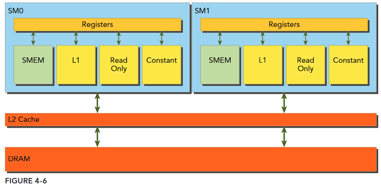
Global memory loads/stores are staged through caches, as shown in Figure 4-6. Global memory is a logical memory space that you can access from your kernel. All application data initially resides in DRAM, the physical device memory. Kernel memory requests are typically served between the device DRAM and SM on-chip memory using either 128-byte or 32-byte memory transactions.
All accesses to global memory go through the L2 cache. Many accesses also pass through the L1 cache, depending on the type of access and your GPU’s architecture. If both L1 and L2 caches are used, a memory access is serviced by a 128-byte memory transaction. If only the L2 cache is used, a memory access is serviced by a 32-byte memory transaction. On architectures that allow the L1 cache to be used for global memory caching, the L1 cache can be explicitly enabled or disabled at compile time.
内存访问事务需要经过 cache
内存传输的宽度也和经过的 cache 有关:L1 & L2: 128-byte;L2 only: 32-byte
An L1 cache line is 128 bytes, and it maps to a 128-byte aligned segment in device memory. If each thread in a warp requests one 4-byte value, that results in 128 bytes of data per request, which maps perfectly to the cache line size and device memory segment size.
There are two characteristics of device memory accesses that you should strive for when optimizing your application:
- Aligned memory accesses. Aligned memory accesses occur when the first address of a device memory transaction is an even multiple of the cache granularity being used to service the transaction (either 32 bytes for L2 cache or 128 bytes for L1 cache). Performing a misaligned load will cause wasted bandwidth.
- Coalesced memory accesses. Coalesced memory accesses occur when all 32 threads in a warp access a contiguous chunk of memory.
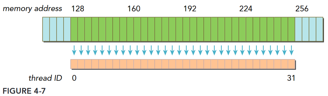
Aligned coalesced memory accesses are ideal: A wrap accessing a contiguous chunk of memory starting at an aligned memory address. To maximize global memory throughput, it is important to organize memory operations to be both aligned and coalesced.
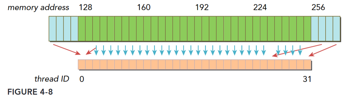
Figure 4-7 illustrates an aligned and coalesced memory load operation. In this case, only a single 128-byte memory transaction is required to read the data from device memory. Figure 4-8 illustrates a misaligned and uncoalesced memory access. In this case, there may be as many as three 128-byte memory transactions to read the data from device memory: one starting at offset 0 to include the data being read below the contiguous region, one at offset 256 to read the data being read above the contiguous region, and one at offset 128 that fetches the bulk of the data. Note that most of the bytes fetched by the lower and upper memory transactions will not be used, leading to wasted bandwidth.
对齐与合并
对齐是访问事务的第一个地址是 cache 粒度的偶数倍。合并是一个 warp 中的 32 个 thread 访问连续的一块。
Global Memory Reads
In an SM, data is pipelined through one of the following three cache/buffer paths, depending on what type of device memory is being referenced:
- L1/L2 cache
- Constant cache
- Read-only cache
Global Memory Access Caching
Compute Capability 5.x states that: Global memory accesses are always cached in L2. And Compute Capability above 5.x behaves the same way as in devices of compute capability 5.x.
Compute Capability 6.x states that: The cache behavior (for example, whether reads are cached in both the unified L1/texture cache and L2 or in L2 only) can be partially configured on a per-access basis using modifiers to the load instruction.
CUDA C++ Best Practice states that: For certain devices of compute capability 5.2, L1-caching of accesses to global memory can be optionally enabled. If L1-caching is enabled on these devices, the number of required transactions is equal to the number of required 128-byte aligned segments. On devices of compute capability 6.0 or higher, L1-caching is the default, however the data access unit is 32-byte regardless of whether global loads are cached in L1 or not.
See also 内存访问解读.
L1/L2 cache is the default path. To pass data through the other two paths requires explicit management by the application, but can lead to performance improvement depending on the access patterns used.
Whether global memory load operations pass through the L1 cache depends on two factors:
- Device compute capability
- Compiler options
On Fermi GPUs (compute capability 2.x) and Kepler K40 or later GPUs (compute capability 3.5 and up), L1 caching of global memory loads can be either enabled or disabled with compiler flags. By default, the L1 cache is enabled for global memory loads on Fermi devices and disabled on K40 and later GPUs. The following flags inform the compiler to disable the L1 cache:
-Xptxas -dlcm=cgWith the L1 cache disabled, all load requests to global memory go directly to the L2 cache; when an L2 miss occurs, the requests are serviced by DRAM. Each memory transaction may be conducted by one, two, or four segments, where one segment is 32 bytes. The L1 cache can also be explicitly enabled with the following flag:
-Xptxas -dlcm=caWith this flag set, global memory load requests first attempt to hit in L1 cache. On an L1 miss, the requests go to L2. On an L2 miss, the requests are serviced by DRAM. In this mode, a load memory request is serviced by a 128-byte device memory transaction.
On Kepler K10, K20, and K20x GPUs, the L1 cache is not used to cache global memory loads. The L1 cache is exclusively used to cache register spills to local memory.
MEMORY LOAD ACCESS PATTERNS
There are two types of memory loads:
- Cached load (L1 cache enabled)
- Uncached load (L1 cache disabled)
The access pattern for memory loads can be characterized by the following combinations:
- Cached versus uncached: The load is cached if L1 cache is enabled
- Aligned versus misaligned: The load is aligned if the first address of a memory access is a multiple of 32 bytes
- Coalesced versus uncoalesced: The load is coalesced if a warp accesses a contiguous chunk of data
访存性能分析
When analyzing kernel performance, it is important to focus on memory latency, the time to satisfy an individual memory request, and memory bandwidth, the rate at which device memory can be accessed by an SM, measured in bytes per time unit.
In the last section, you experimented with two methods for improving kernel performance:
- Hiding memory latency by maximizing the number of concurrently executing warps, leading to better saturation of the bus by keeping more memory accesses in-flight.
- Maximizing memory bandwidth efficiency by properly aligning and coalescing memory accesses.
核心优化点
内核性能:
- 内存延迟——通过最大化并发执行的线程束数量隐藏内存延迟,增加在途内存访问以更好地饱和总线
- 内存带宽——通过合理对齐和合并内存访问,最大化内存带宽效率
面临的关键问题:
- 当问题本身存在固有不良访问模式时,内核性能“足够好”的标准是什么?
- 非最优场景下可实现的最佳性能水平如何?
Memory Bandwidth
Most kernels are very sensitive to memory bandwidth, that is, they are memory bandwidth-bound. As a result, it is often important to focus on memory bandwidth metrics while tuning kernels. Bandwidth can be dramatically affected by how data in global memory is arranged, and how that data is accessed by a warp. There are two types of bandwidth:
- Theoretical bandwidth. Theoretical bandwidth is the absolute maximum bandwidth achievable with the hardware at hand. For a Fermi M2090 with ECC disabled, the peak theoretical device memory bandwidth is 177.6 GB/s.
- Effective bandwidth. Effective bandwidth is the measured bandwidth that a kernel actually achieves, and is calculated using the following equation:
For example, for a copy of a matrix containing 4-byte integers to and from the device, the effective bandwidth can be computed with the following formula:
Case Study: Matrix Transpose Problem
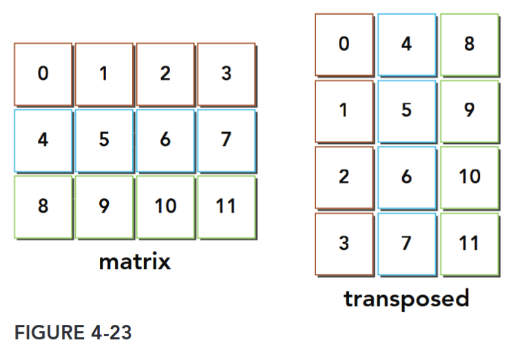
共享内存和常量内存
参考: Professional CUDA C Programming 第 5 章。重点:
- Learning how data is arranged in shared memory
- Mastering index conversion from 2D shared memory to linear global memory
- Resolving bank conflicts for different access modes
- Caching data in shared memory to reduce global memory accesses
- Avoiding non-coalesced global memory access using shared memory
- Understanding the difference between the constant cache and the read-only cache
- Programming with the warp shuffle instruction 本章将会介绍两个例子:规约和矩阵转置。
Shared Memory
Misaligned memory accesses are not as problematic since modern GPU hardware includes an L1 cache, but non-coalesced memory accesses that stride through global memory still cause suboptimal bandwidth utilization. However, it is possible to improve global memory coalesced access using shared memory in many cases.
GPUs are equipped with two types of memory:
- On-board memory
- On-chip memory
Global memory is large, on-board memory and is characterized by relatively high latencies. Shared memory is smaller, low-latency on-chip memory that offers much higher bandwidth than global memory. You can think of it as a program-managed cache. Shared memory is generally useful as:
- An intra-block thread communication channel
- A program-managed cache for global memory data
- Scratch pad memory for transforming data to improve global memory access patterns
共享内存
Shared memory (SMEM) is one of the key components of the GPU. Physically, each SM contains a small low-latency memory pool shared by all threads in the thread block currently executing on that SM. Shared memory enables threads within the same thread block to cooperate, facilitates reuse of on-chip data, and can greatly reduce the global memory bandwidth needed by kernels. Because the contents of shared memory are explicitly managed by the application, it is often
described as a program-managed cache.
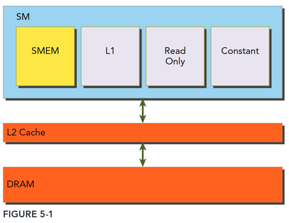
As illustrated in Figure 5-1, all load and store requests to global memory go through the L2 cache, which is the primary point of data unification between SM units. Note that shared memory and L1 cache are physically closer to the SM than both the L2 cache and global memory. As a result, shared memory latency is roughly 20 to 30 times lower than global memory, and bandwidth is nearly 10 times higher.
- A fixed amount of shared memory is allocated to each thread block when it starts executing.
- This shared memory address space is shared by all threads in a thread block.
- Its contents have the same lifetime as the thread block in which it was created.
- Shared memory accesses are issued per warp. Ideally, each request to access shared memory by a warp is serviced in one transaction.
Shared memory is partitioned among all resident thread blocks on an SM; therefore, shared memory is a critical resource that limits device parallelism. The more shared memory used by a kernel, the fewer possible concurrently active thread blocks.
共享内存仍要经过 L2 Cache,使用规则与“线程块(Thread Block)”强绑定,是线程块内线程协作的关键,而访问粒度与 warp 绑定,内存由 SM 驻留的所有 Block 分配。
分配
There are several ways to allocate or declare shared memory variables depending on your application requirements. You can allocate shared memory variables either statically or dynamically. Shared memory can also be declared as either local to a CUDA kernel or globally in a CUDA source code file. CUDA supports declaration of 1D, 2D, and 3D shared memory arrays.
// inside or outside of a kernel
__shared__ float tile[size_y][size_x];

// dynamically declare an array (only 1D) and specify the size
extern __shared__ int tile[];
kernel<<<grid, block, isize*sizeof(int)>>>(...);
在 CUDA 中,
__shared__变量在核函数外部声明时,其作用域是全局的(对同一编译单元内的所有核函数可见),但这并不改变共享内存的本质特性 —— 它仍然是每个线程块(block)私有的内存。
访问
There are two key properties to measure when optimizing memory performance: latency and bandwidth. different global memory access patterns impact kernel performance of latency and bandwidth. Shared memory can be used to hide the performance impact of global memory latency and bandwidth. To fully exploit these resources, it is helpful to understand how shared memory is arranged.
Memory Banks
32 Memory Banks
To achieve high memory bandwidth, shared memory is divided into 32 equally-sized memory modules, called banks, which can be accessed simultaneously.
There are 32 banks because there are 32 threads in a warp. Shared memory is a 1D address space. Depending on the compute capability of a GPU, the addresses of shared memory are mapped to different banks in different patterns (more on this later). If a shared memory load or store operation issued by a warp does not access more than one memory location per bank, the operation can be serviced by one memory transaction. Otherwise, the operation is serviced by multiple memory transactions, thereby decreasing memory bandwidth utilization.
Bank Conflict
Bank Conflict
Multiple addresses in a shared memory request fall into the same memory bank, causing the request to be replayed.
The hardware splits a request with a bank conflict into as many separate conflict-free transactions as necessary, decreasing the effective bandwidth by a factor equal to the number of separate memory transactions required.
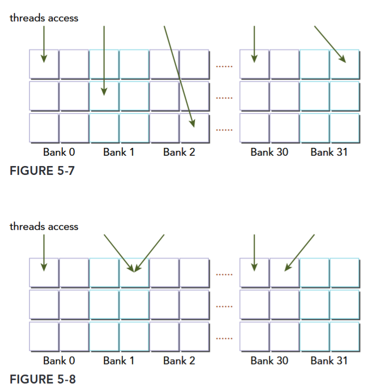
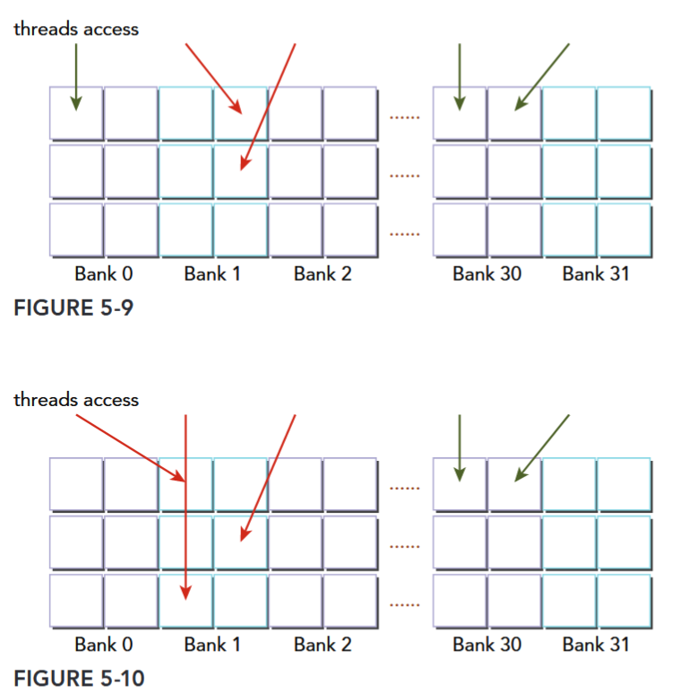
Three typical situations occur when a request to shared memory is issued by a warp:
- Parallel access: multiple addresses accessed across multiple banks
- Serial access: multiple addresses accessed within the same bank
- Broadcast access: a single address read in a single bank
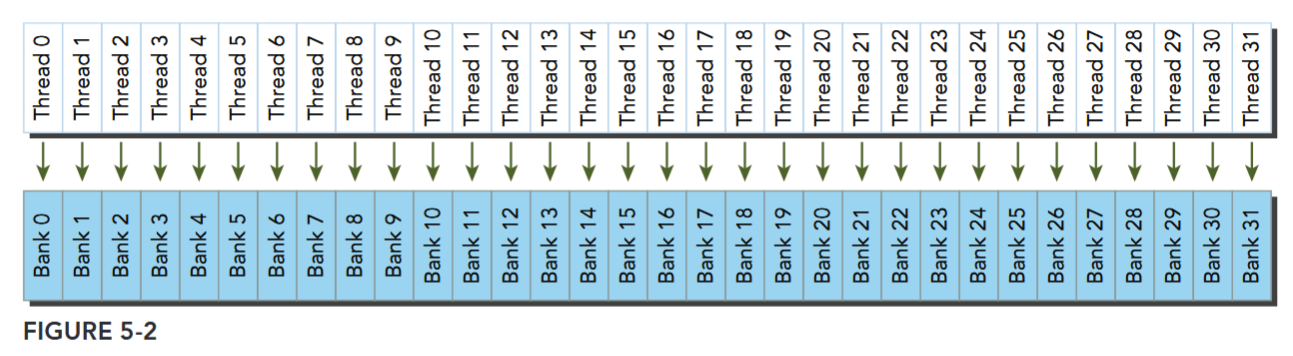
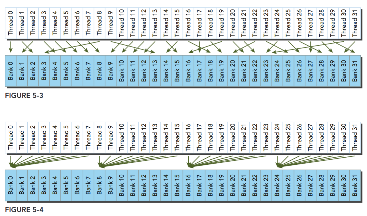
Fig 5-2、5-3 都是规则和不规则的无冲突访存,Fig 5-4 可能是不冲突的广播,可能出现冲突。
Access Mode
Shared memory bank width defines which shared memory addresses are in which shared memory banks. Memory bank width varies for devices depending on compute capability.
There are two different bank widths:
- 4 bytes (32-bits) for devices of compute capability 2.x
- 8 bytes (64-bits) for devices of compute capability 3.x
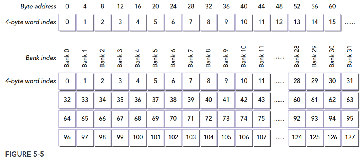
For a Fermi device, the bank width is 32-bits and there are 32 banks. Each bank has a bandwidth of 32 bits per two clock cycles. Successive 32-bit words map to successive banks. Hence, the mapping from shared memory address to bank index can be calculated as follows:
The byte address is divided by 4 to convert to a 4-byte word index, and the modulo 32 operation converts the 4-byte word index into a bank index.
The top of Figure 5-5 illustrates the mapping from byte address to word index for Fermi devices. At the bottom, the mapping from word index to bank index is shown. Note that bank membership wraps around every 32 words. Neighboring words are classified in different banks to maximize the number of possible concurrent accesses for a warp.
A bank conflict does not occur when two threads from the same warp access the same address. In that case, for read accesses, the word is broadcast to the requesting threads, and for write accesses, the word is written by only one of the threads — which thread performs the write is undefined.
对于 Kepler 架构,带宽是 64bit/cycle,64 位的地址相应计算同理。只读一个 32-bit word 是可以的,这时一个 Bank 容纳两个 32-bit word,所以同时访问这两个 word 不会冲突。
不会冲突:
两路冲突和三路冲突:
用于共享内存访存位宽的访存模式配置的 API cudaDeviceSetSharedMemConfig cudaSharedMemConfig 已被弃用。
Configuring the Amount of Shared Memory
The shared memory and L1 cache share this hardware resource. CUDA provides two methods for configuring the size of L1 cache and shared memory:
- Per-device configuration
- Per-kernel configuration
You can configure how much L1 cache and how much shared memory will be used by kernels launched on a given device with the following runtime function:
__host__ cudaError_t cudaDeviceSetCacheConfig ( cudaFuncCache cacheConfig )
/*
Sets the preferred cache configuration for the current device.
###### Parameters
cacheConfig
- Requested cache configuration
*/The argument cacheConfig specifies how on-chip memory should be partitioned between the L1 cache and shared memory on the current CUDA device. The supported cache configurations are (See also cudaFuncCache):
enum cudaFuncCache

// CUDA function cache configurations
// Values

cudaFuncCachePreferNone = 0
// Default function cache configuration, no preference

cudaFuncCachePreferShared = 1
// Prefer larger shared memory and smaller L1 cache

cudaFuncCachePreferL1 = 2
// Prefer larger L1 cache and smaller shared memory

cudaFuncCachePreferEqual = 3
// Prefer equal size L1 cache and shared memory
在 Professional C Programming Guide 中提到 register spill 在 Kepler 架构是用 L1 Cache,Fermi 架构是 local memory 但是会在 L1 Cache 暂存,Device Memory Accesses 表明:Any variable if the kernel uses more registers than available (this is also known as register spilling)。CUDA 13 register spilling(Aug 27, 2025) 提出用 shared memory。
The CUDA runtime makes a best effort to use the requested device on-chip memory configuration, but it is free to choose a different configuration if required to execute a kernel function. A per-kernel configuration can also override the device-wide setting, and can be set using the following runtime function:
__host__ cudaError_t cudaFuncSetCacheConfig ( const void* func, cudaFuncCache cacheConfig )
/*
Sets the preferred cache configuration for a device function.
###### Parameters
func
- Device function symbol
cacheConfig
- Requested cache configuration
*/Essence of Cache and Shared Memory
Even though L1 cache and shared memory are located in the same on-chip hardware, several things are quite different between them. Shared memory is accessed through 32 banks, while L1 cache is accessed by cache line. With shared memory, you have full control over what gets stored and where, while with L1 cache, data eviction is done by the hardware.
GPU CACHE VERSUS CPU CACHE
In general, GPU cache behavior is more difficult to reason about than CPU cache behavior. The GPU uses different heuristic algorithms to evict data. On GPUs, hundreds of threads share the same L1 cache, and thousands of threads share the same L2 cache; therefore, data eviction might occur more often and unpredictably on a GPU. You can use GPU shared memory to explicitly manage data and guarantee locality to an SM.
Synchronization
CUDA provides several runtime functions to perform intra-block synchronization. In general, there are two basic approaches to synchronization:
- Barriers
- Memory fences
At a barrier, all calling threads wait for all other calling threads to reach the barrier point. At a memory fence, all calling threads stall until all modifications to memory are visible to all other calling threads.
Weakly-Ordered Memory Model
Modern memory architectures have a relaxed memory model. This means that the memory accesses are not necessarily executed in the order in which they appear in the program. CUDA adopts a weakly-ordered memory model to enable more aggressive compiler optimizations.
- The order in which a GPU thread writes data to different memories, such as shared memory, global memory, page-locked host memory, or the memory of a peer device, is not necessarily the same order of those accesses in the source code.
- The order in which a thread’s writes become visible to other threads may not match the actual order in which those writes were performed.
- The order in which a thread reads data from different memories is not necessarily the order in which the read instructions appear in the program if instructions are independent of each other.
To explicitly force a certain ordering for program correctness, memory fences and barriers must be inserted in application code. This is the only way to guarantee the correct behavior of a kernel that shares resources with other threads.
Explicit Barrier
Barrier
CUDA’s
__syncthreads()synchronizes threads within a block, requiring all to reach the same barrier point.
You can specify a barrier point in a kernel by calling the following intrinsic function (See also Synchronization Functions:
void __syncthreads();__syncthreadsacts as a barrier point at which threads in a block must wait until all threads have reached that point.__syncthreadsalso ensures that all global and shared memory accesses made by these threads prior to the barrier point are visible to all threads in the same block.
__syncthreads is used to coordinate communication between the threads of the same block. When some threads within a block access the same addresses in shared or global memory, there are potential hazards (read-after-write, write-after-read, and write-after-write) which will result in undefined application behavior and undefined state at those memory locations. This undesirable behavior can be avoided by synchronizing threads between conflicting accesses.
You must be particularly careful when using __syncthreads in conditional code. It is only valid to call __syncthreads if a conditional is guaranteed to evaluate identically across the entire thread block. Otherwise execution is likely to hang or produce unintended side effects. For example, the following code segment may cause threads in a block to wait indefinitely for each other because all threads in a block never hit the same barrier point.
if (threadID % 2 == 0) { __syncthreads(); }
else { __syncthreads(); }线程块内的线程并非全部到达同一个
__syncthreads()调用点(而是分散在两个不同的分支里)。两类线程永远等不到对方到达自己所在的同步点,最终导致线程死锁(程序卡住,无法继续执行)。
By not allowing synchronization across blocks, thread blocks can be executed in any order, in parallel or in series, on any SM. This independent nature of block execution makes CUDA programming scalable across an arbitrary number of cores.
If a CUDA kernel requires global synchronization across blocks, you can likely achieve the desired behavior by splitting the kernel apart at the synchronization point and performing multiple kernel launches. Because each successive kernel launch must wait for the preceding kernel launch to complete, this produces an implicit global barrier.
Memory Fence
Memory fence
Memory fence functions ensure that any memory write before the fence is visible to other threads after the fence.
There are three variants of memory fences depending on the desired scope: block, grid, or system (See Also Memory fence Functions).
- You can create a memory fence within a thread block using the following intrinsic function:
void __threadfence_block()ensures that all writes to shared memory and global memory made by a calling thread before the fence are visible to other threads in the same block after the fence. Recall that memory fences do not perform any thread synchronization, and so it is not necessary for all threads in a block to actually execute this instruction. - You can create a memory fence at the grid level using the following intrinsic function:
void __threadfence()stalls the calling thread until all of its writes to global memory are visible to all threads in the same grid. - You can also set a memory fence across the system (including host and device) using the following intrinsic function:
void __threadfence_system()stalls the calling thread to ensure all its writes to global memory, page-locked host memory, and the memory of other devices are visible to all threads in all devices and host threads.
现代 CPU 普遍采用强内存模型,硬件保证大部分内存一致性,CPU 硬件通过缓存一致性协议自动同步缓存,而在一些弱内存模型 CPU 中,弱代码有复杂依赖可能需要 fence,但日常开发通常已经封装了这些操作。 GPU 是弱内存模型,硬件无法保证高效的内存一致性。 内存栅栏函数侧重于内存一致性,解决不同线程对内存读写的可见性问题,防止因内存访问顺序和可见性不一致导致的程序错误。
Volatile Qualifier
Declaring a variable in global or shared memory using the volatile qualifier prevents compiler optimization which might temporally cache data in registers or local memory. With the volatile qualifier, the compiler assumes that the variable’s value can be changed or used at any time by any other thread. Therefore, any reference to this variable is compiled to a global memory read or global memory write instruction that skips the cache.
THE WARP SHUFFLE INSTRUCTION
Variants of the Warp Shuffle Instruction
- The shuffle instruction enables threads in a warp to exchange data with each other directly, rather than going through shared or global memory. The shuffle instruction has lower latency than shared memory and does not consume extra memory to perform a data exchange.
- A lane simply refers to a single thread within a warp. Each lane in a warp is uniquely identified by a lane index in the range
[0,31].- In a 1D thread block, the lane index and warp index for a given thread can be calculated as:
laneID = threadIdx.x % 32 warpID = threadIdx.x / 32.
- In a 1D thread block, the lane index and warp index for a given thread can be calculated as:
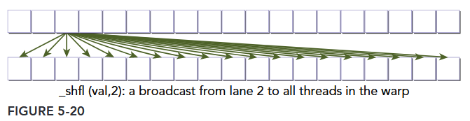
- There are two sets of shuffle instructions: one for integer variables and another for float variables. Each set has four variants of the shuffle instruction. To exchange integer variables within a warp, the basic function signature is as follows:
int __shfl(int var, int srcLane, int width=warpSize);The intrinsic instruction __shfl returns the value var passed to __shfl by the thread in the same warp identified by srcLane. The meaning of srcLane changes depending on the value of width. This function makes it possible for each thread in a warp to directly fetch a value from a specific thread. This operation occurs simultaneously for all active threads within a warp, moving 4 bytes of data per thread.
shuffle指令允许 warp 中的 thread 直接交换数据。注:指令的含义会随
width变化,如下所说。
Optionally, the variable width can be set to any power-of-2 between 2 and 32, inclusive.
- When set to the default warpSize (that is, 32) a shuffle instruction is performed across the entire warp and srcLane specifies the lane index of the source thread.
- However, setting width permits subdivision of a warp into segments containing width threads each, with a separate shuffle operation performed in each segment. For values of width other than 32, the lane ID of a thread and its ID in a shuffle operation are not necessarily equal. In that case, the shuffle ID of a thread in a 1D thread block can be calculated as:
shuffleID = threadIdx.x % width;
For example, if shfl were called from every thread in a warp with the following arguments:
int y = shfl(x, 3, 16);
Then threads 0 through 15 would receive the value of x from thread 3, and threads 16 through 31 would receive the value of x from thread 19 (the thread with offset 3 in the top 16 threads of the warp). For simplicity, srcLane will be referred to as a lane index for the remainder of this section. When the lane index passed to shfl is the same value for all threads in a warp, the instruction performs a warp broadcast operation from the specified lane to all threads in the warp, as illustrated in Figure 5-20.
Another variant of the shuffle operation copies data from a thread identified relative to the calling thread:
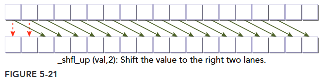
int __shfl_up(int var, unsigned int delta, int width=warpSize)
__shfl_up calculates the source lane index by subtracting delta from the caller’s lane index. The value held by the source thread is returned. Hence, this instruction shifts var up the warp by delta lanes. There is no wrap around with __shfl_up, so the lowest delta threads in a warp will be unchanged, as illustrated in Figure 5-21.
The third variant of the shuffle instruction instead copies from a thread with higher index relative to the calling thread:
int __shfl_down(int var, unsigned int delta, int width=warpSize)
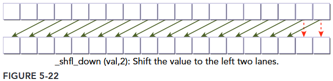
__shfl_down calculates a source lane index by adding delta to the caller’s lane index. The value held by the source thread is returned. Hence, this instruction shifts var down the warp by delta lanes. There is no wrap around when using __shfl_down, so the upper delta lanes in a warp will remain unchanged, as illustrated in Figure 5-22.
The last variant of the shuffle instruction transfers data from a lane based on a bitwise XOR of the caller’s own lane index:
int __shfl_xor(int var, int laneMask, int width=warpSize)
The intrinsic instruction calculates a source lane index by performing a bitwise XOR of the caller’s lane index with laneMask. The value held by the source thread is returned. This instruction facilitates a butterfly addressing pattern, as illustrated in Figure 5-23.
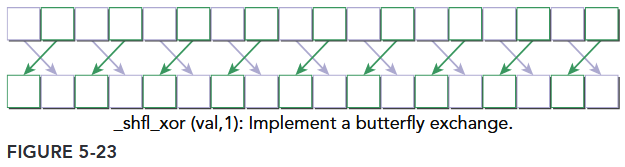
注,这条指令的源通道索引计算为: src_lane = lane_id ^ laneMask。
- 若当前线程是通道 0(
lane_id=0),则src_lane = 0 ^ 1 = 1→ 获取通道 1 的val。 - 若当前线程是通道 1(
lane_id=1),则src_lane = 1 ^ 1 = 0→ 获取通道 0 的val。 - 若当前线程是通道 2(
lane_id=2),则src_lane = 2 ^ 1 = 3→ 获取通道 3 的val。 - 以此类推,所有偶数编号通道(0、2、4…)会与下一个奇数编号通道(1、3、5…)互换数据。
__shfl_xor 非常适合实现蝶形数据交换模式,这在快速傅里叶变换(FFT)、归约(Reduction)等算法中广泛使用。例如,以下代码演示了线程束内基于蝶形模式的数据交换(以 width=8 为例):
__global__ void butterflyShuffle(int *data) {
    int lane_id = threadIdx.x % 8;  // 假设width=8,通道索引0~7
    int value = data[threadIdx.x];

    // 逐步扩大掩码,实现蝶形交换
    for (int mask = 1; mask < 8; mask <<= 1) {
        int neighbor_value = __shfl_xor(value, mask, 8);
        value += neighbor_value;  // 示例:累加相邻线程的数据
    }

    data[threadIdx.x] = value;
}- 以
lane_id=0为例:- 当
mask=1时,src_lane = 0 ^ 1 = 1→ 与通道 1 交换数据。 - 当
mask=2时,src_lane = 0 ^ 2 = 2→ 与通道 2 交换数据。 - 当
mask=4时,src_lane = 0 ^ 4 = 4→ 与通道 4 交换数据。
- 当
通过这种模式,线程可以高效地与距离逐渐扩大的 “邻居” 线程交换数据,无需共享内存或全局内存,大幅提升计算效率。
Sharing Data within a Warp
Shuffle instructions will be applied to the following three integer variable types:
- Scalar variable
- Array
- Vector-typed variable